
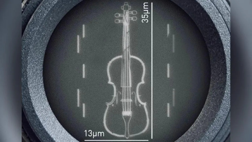
Scientists from Loughborough University in the UK have created the smallest in the world a violin measuring only 35 microns.
It is noted that it is thinner than a human hair and is made of platinum, which was etched on a silicon chip with incredible precision. This achievement paves the way for deeper scientific research into nanoscale materials.
«While building the world’s smallest violin may seem like a fun and exciting activity, much of what we learned in the process actually laid the foundation for the research we are currently conducting», — explains the project leader, a physicist Kelly Morrison.
Under the microscope, you can see clear lines and curves, as well as incredible proportions. To the naked eye, it looks like a tiny speck. Interestingly, a device the size of an entire room was needed to create the world’s smallest musical instrument. This device is called NanoFrazor.
The chip was covered with two layers of gel-like material — resist. An ultra-thin, needle-like tip etched a violin shape on the top layer using a technique called thermal scanning probe lithography. The gel at this time evaporated, leaving microscopic depressions in the shape of a violin.
The researchers then dissolved the substrate to create the mold. They then applied a thin platinum film to the remaining cavities and finally removed the residue with acetone. In this way, they obtained an incredibly tiny platinum violin.
Each image takes about 3 hours to create. However, the final version of the instrument took more than a month to complete, with a lot of trial and error. This was the first result from Loughborough’s powerful new nanolithography system, which allows scientists to create nanoscale materials.
«Our nanolithography system allows us to design experiments in which materials are examined in different ways — using light, magnetism or electricity — and observe their reaction. Once we understand how materials behave, we can start applying this knowledge to develop new technologies, whether it’s improving the efficiency of computing or finding new ways to generate energy», — adds Kelly Morrison.
This will allow scientists to study the behavior of different nanoscale materials, that will serve as the basis for the next generation of electronic devices. These devices will be smaller and consume significantly less electricity.
World’s smallest semiconductor structure used to produce «pure» hydrogen
Source: ZMEScience
Spelling error report
The following text will be sent to our editors: